- 您现在的位置:买卖IC网 > Sheet目录252 > SMP3V3-M3/85A (Vishay General Semiconductor)TVS 400W UNIDIR 3.3V SMP
SMP3V3 thru SMP36A
www.vishay.com
RATINGS AND CHARACTERISTICS CURVES
(T A = 25 °C unless otherwise noted)
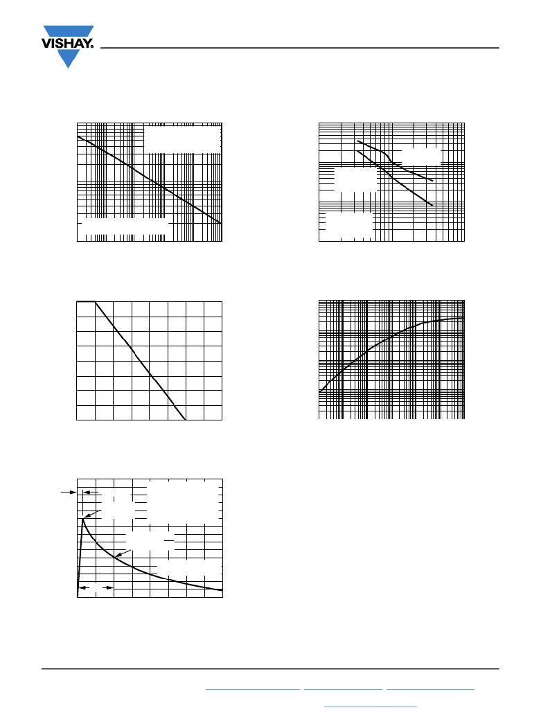
10
N on-Repetitive P u lse
Waveform shown in Fig. 3
10 000
Vishay General Semiconductor
1
T A = 25 °C
1000
100
Meas u red at
Stand-Off
V oltage, V WM
Meas u red at
Zero Bias
0.1
0.2" x 0.2" (5.0 mm x 5.0 mm)
Copper Pad Areas
10
T J = 25 °C
f = 1.0 MHz
V sig = 50 m V p-p
0.1
1
10
100
1000
10 000
1
10
100
100
75
50
25
0
t d - P u lse Width (μs)
Fig. 1 - Peak Pulse Power Rating Curve
1000
100
10
1
0.1
V WM - Reverse Stand-Off V oltage ( V )
Fig. 4 - Typical Junction Capacitance
0
25
50
75
100
125
150
175
200
0.001
0.01
0.1
1
10
100
1000
T J - Initial Temperat u re (°C)
Fig. 2 - Pulse Derating Curve
t - P u lse D u ration (s)
Fig. 5 - Typical Transient Thermal Impedance
150
100
t r = 10 μs
Peak V al u e
I PPM
T J = 25 °C
P u lse Width (t d )
is defined as the Point
where the Peak C u rrent
decays to 50 % of I PPM
?
?
Half V al u e - I PP
50
I PPM
2
10/1000 μs Waveform
as defined by R.E.A.
t d
0
0
1.0
2.0
3.0
4.0
t - Time (ms)
Fig. 3 - Pulse Waveform
Revision: 10-Dec-13
3
Document Number: 88481
For technical questions within your region: DiodesAmericas@vishay.com , DiodesAsia@vishay.com , DiodesEurope@vishay.com
THIS DOCUMENT IS SUBJECT TO CHANGE WITHOUT NOTICE. THE PRODUCTS DESCRIBED HEREIN AND THIS DOCUMENT
ARE SUBJECT TO SPECIFIC DISCLAIMERS, SET FORTH AT www.vishay.com/doc?91000
发布紧急采购,3分钟左右您将得到回复。
相关PDF资料
SMPC8.0A-M3/86A
TVS 1.5KW UNIDIR 8.0V 5% SMPC
SMS12.TCT
IC TVS ARRAY 4-UNI 12V SOT23-6
SMS12C.TCT
IC TVS ARRAY5UNI/2BI 12V SOT23-6
SMS24CT1
TVS ARRAY 5LINE 350W SC74-6
SMS24T1
TVS ARRAY QUAD 350W SC74-6
SMX500RT1U
UPS 500VA 300W 7OUT USB RS232 1U
SN-3700
BOX NEMA METAL W/MB 6X4X3"
SNB-3731SS
BOX NEMA S-STEEL 11.81X9.84X5.91
相关代理商/技术参数
SMP3V3-M3-84A
制造商:VISHAY 制造商全称:Vishay Siliconix 功能描述:Surface Mount TRANSZORB Transient Voltage Suppressors
SMP3V3-M3-85A
制造商:VISHAY 制造商全称:Vishay Siliconix 功能描述:Surface Mount TRANSZORB Transient Voltage Suppressors
SMP3X106KBNMBGA
功能描述:电磁干扰滤波器 100VDC BX CERAMIC HIGH SPEED CAPACITOR RoHS:否 制造商:STMicroelectronics 电容:12 pF 电路类型: 最大直流电流: 最大直流电阻: 电压额定值:6 V 容差: 端接类型:SMD/SMT 工作温度范围:- 30 C to + 85 C 系列:EMIF03
SMP3X336KANMBHR
功能描述:电磁干扰滤波器 50VDC BX CERAMIC HIGH SPEED CAPACITOR RoHS:否 制造商:STMicroelectronics 电容:12 pF 电路类型: 最大直流电流: 最大直流电阻: 电压额定值:6 V 容差: 端接类型:SMD/SMT 工作温度范围:- 30 C to + 85 C 系列:EMIF03
SMP400G-BA
制造商:SEME-LAB 制造商全称:Seme LAB 功能描述:P.I.N. PHOTODIODE
SMP400G-BB
制造商:SEME-LAB 制造商全称:Seme LAB 功能描述:P.I.N. PHOTODIODE
SMP400G-BC
制造商:SEME-LAB 制造商全称:Seme LAB 功能描述:P.I.N. PHOTODIODE
SMP400G-BD
制造商:SEME-LAB 制造商全称:Seme LAB 功能描述:P.I.N. PHOTODIODE
